Intel, AMD, Toshiba 8085 Die Shots
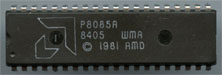
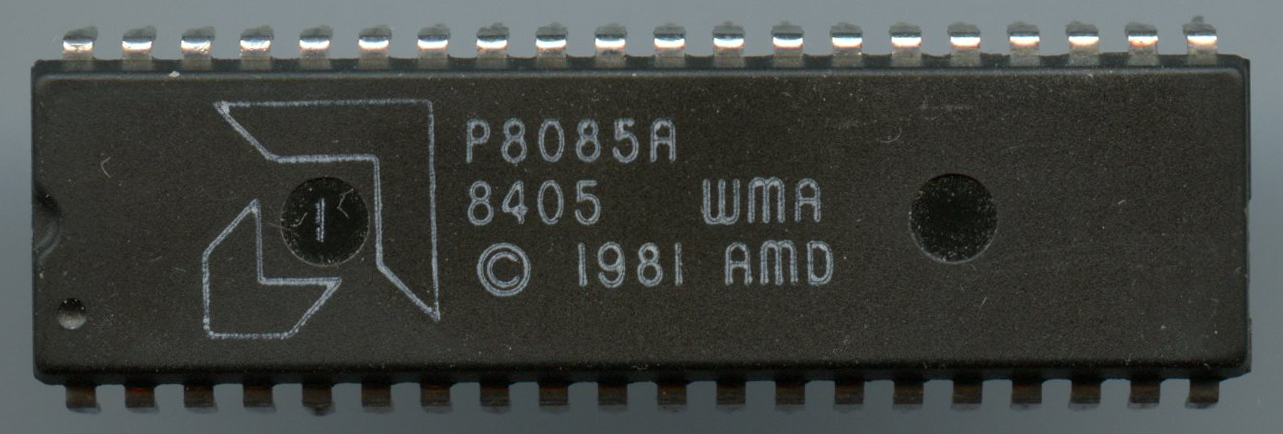
We've depackaged and are preparing die shots of an AMD 8085, Intel 8085, and Toshiba 8085. Thanks to Christian Sattler for delayering and photographing the substrate of the AMD 8085. Curiously, AMD printed 9085 on the die.
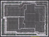
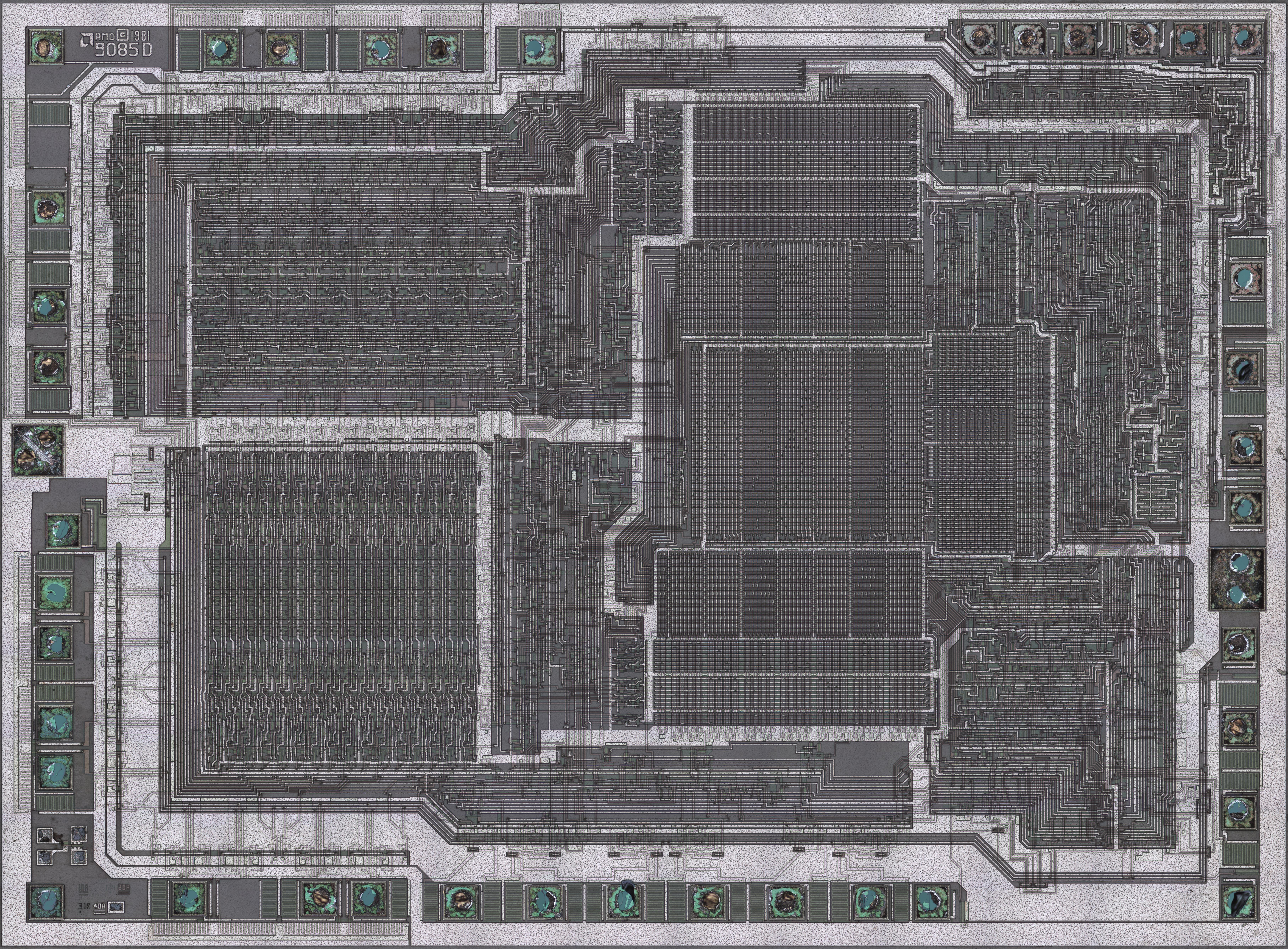
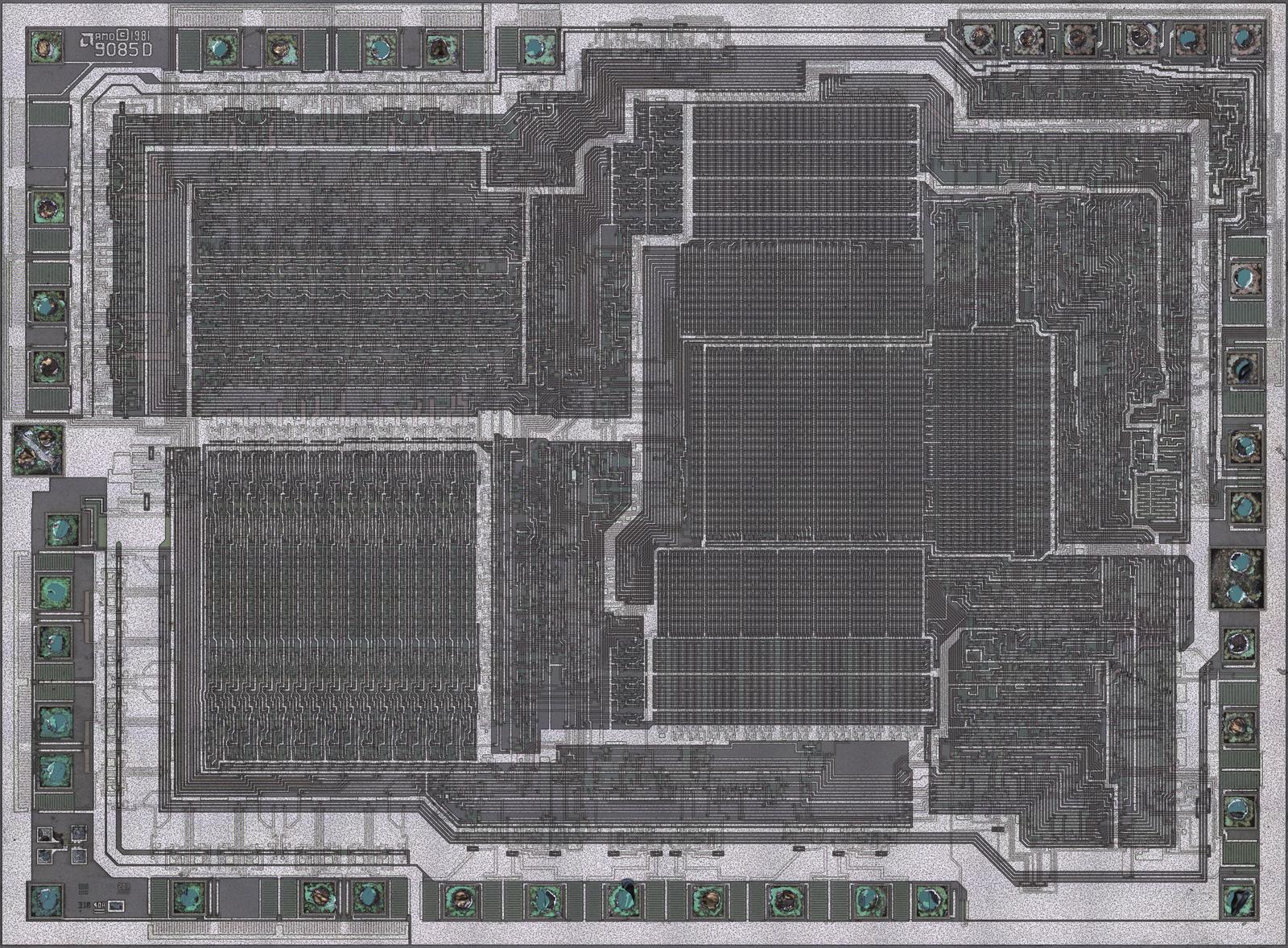
Here's our initial shot of the surface of the AMD 8085/9085
| | 1600 x 1192 JPG 631 kb |
|
|
| | 8000 x 5858 JPG 12.1 MB |
|
The AMD 8085 was depackaged 4/11/2011 and photographed by Greg James in San Francisco, California, using a Nikon LV150 with an LU Plan Fluor 20x objective. Images were then transmitted to the UK where Christian Sattler corrected and stitched them using a combination of
Autopano-sift-C and custom code. The full resolution die shot is 15275 x 11416 pixels.
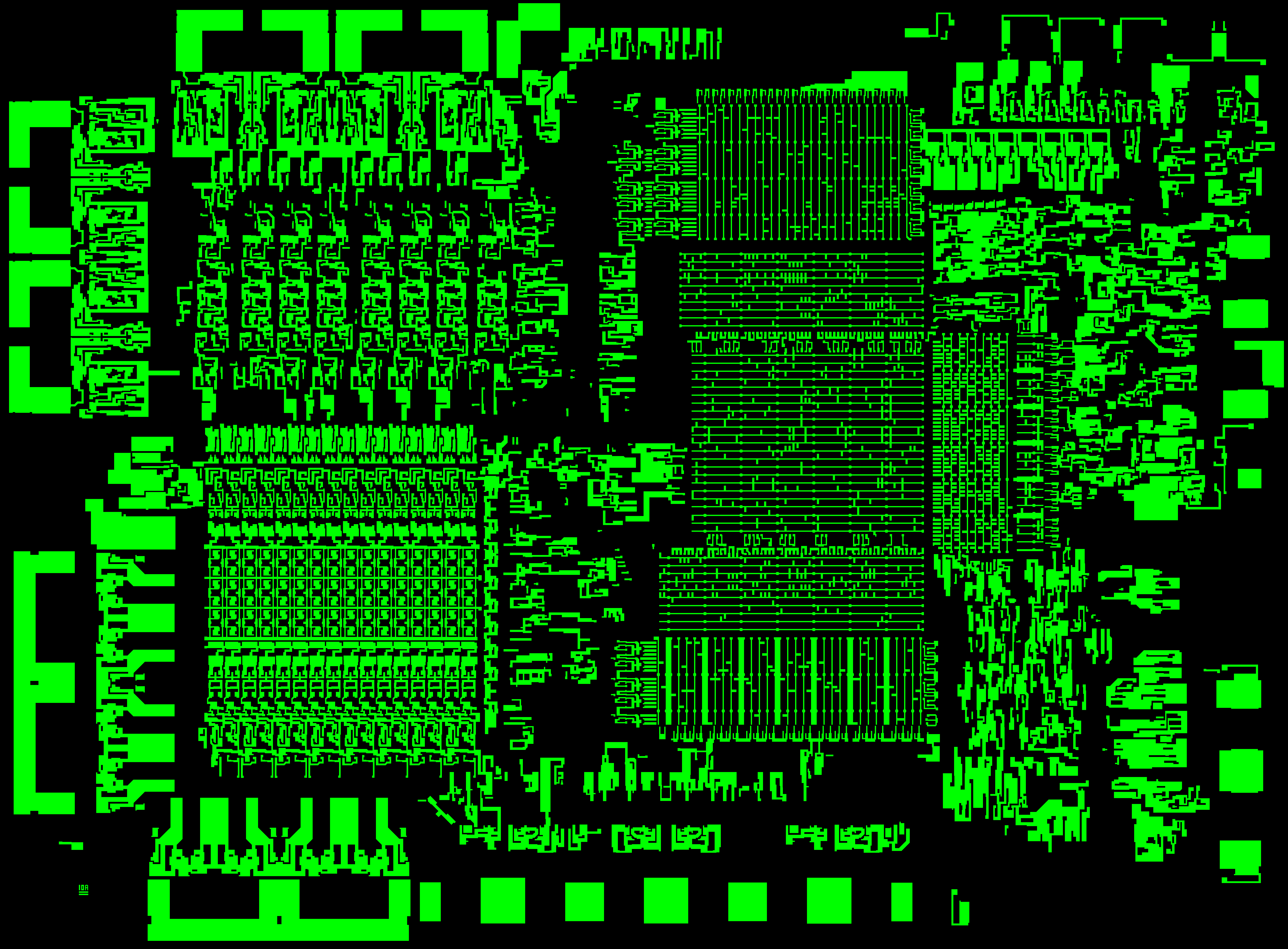
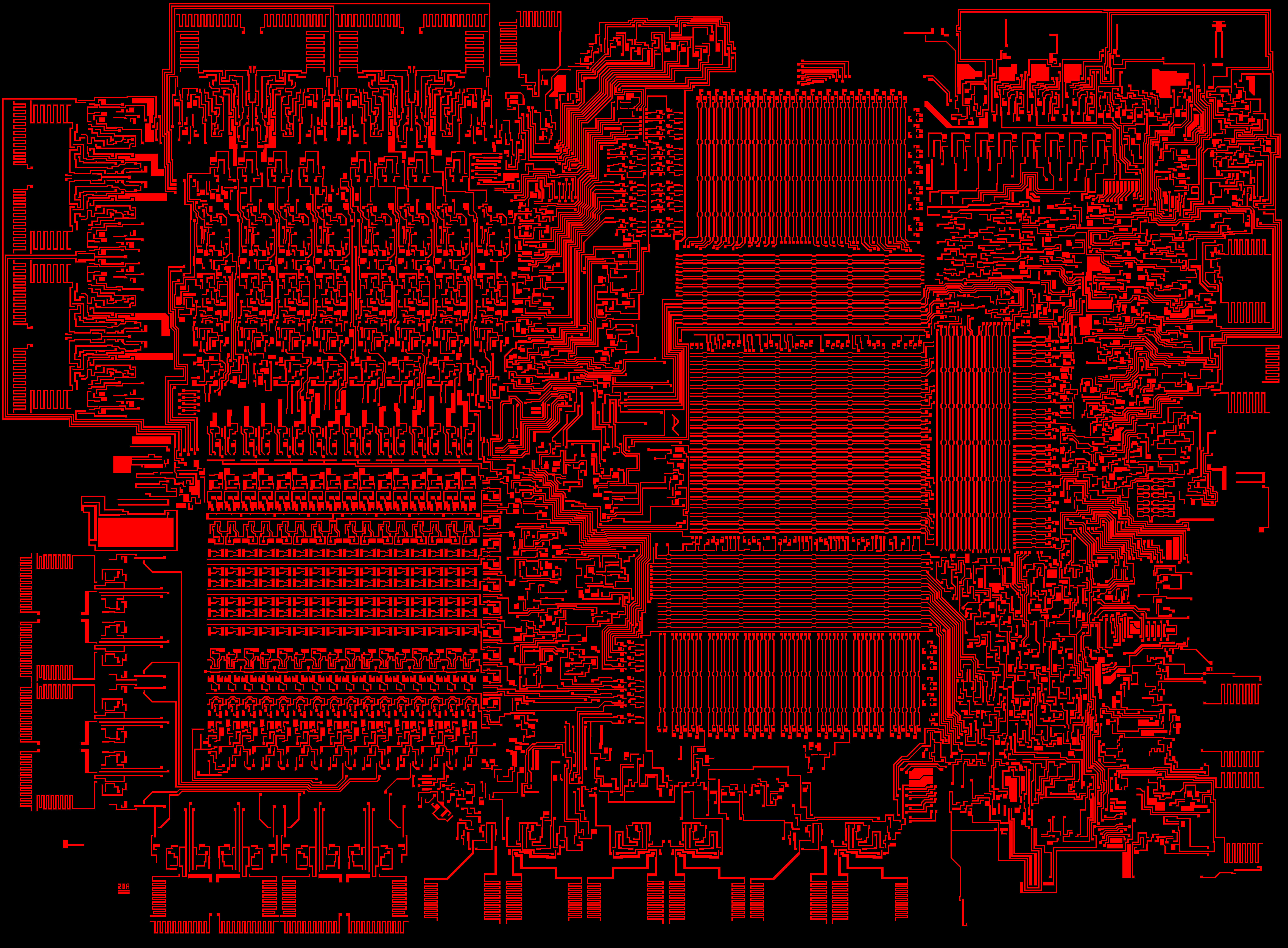
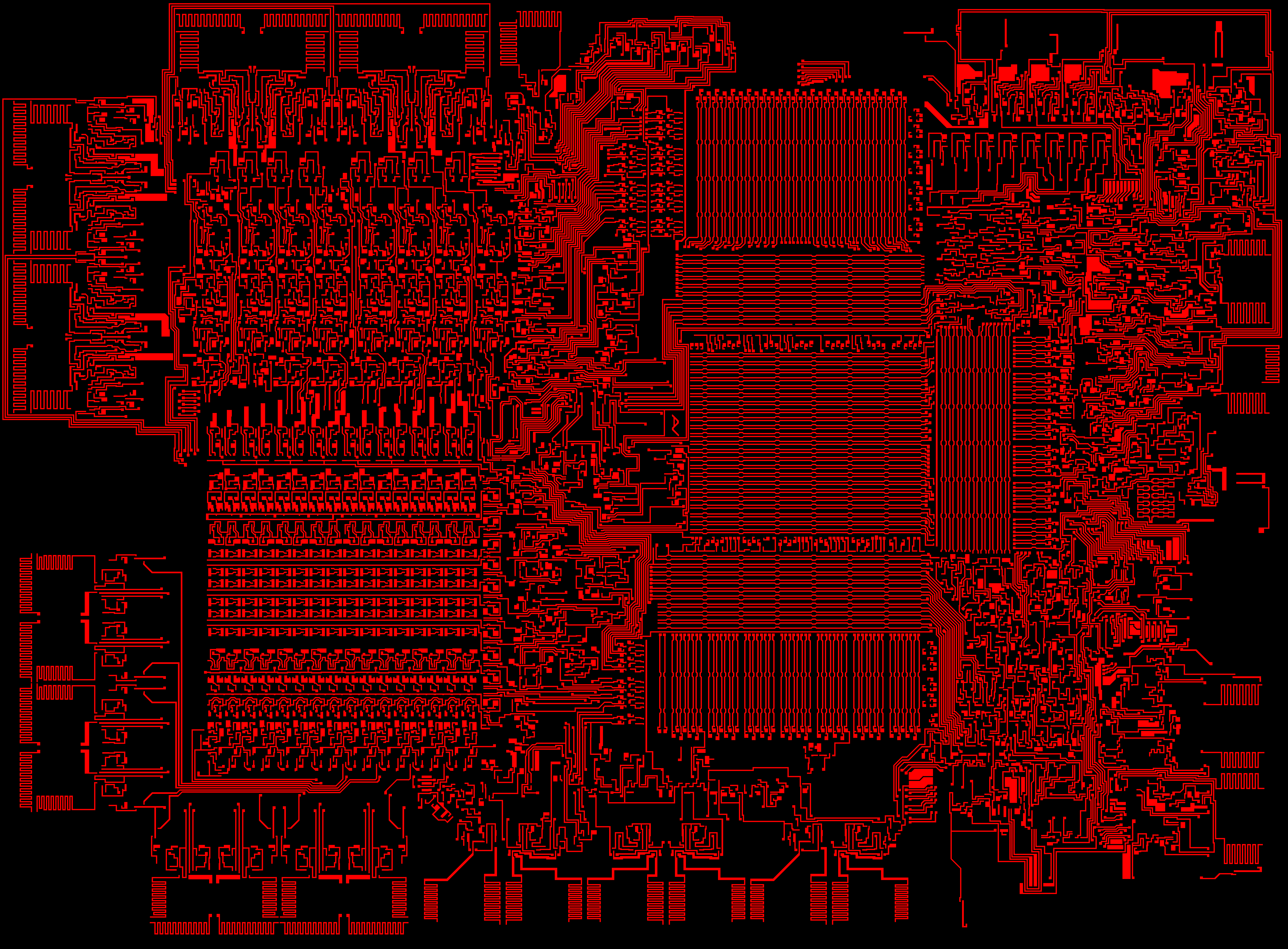
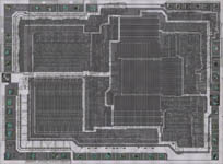
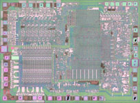
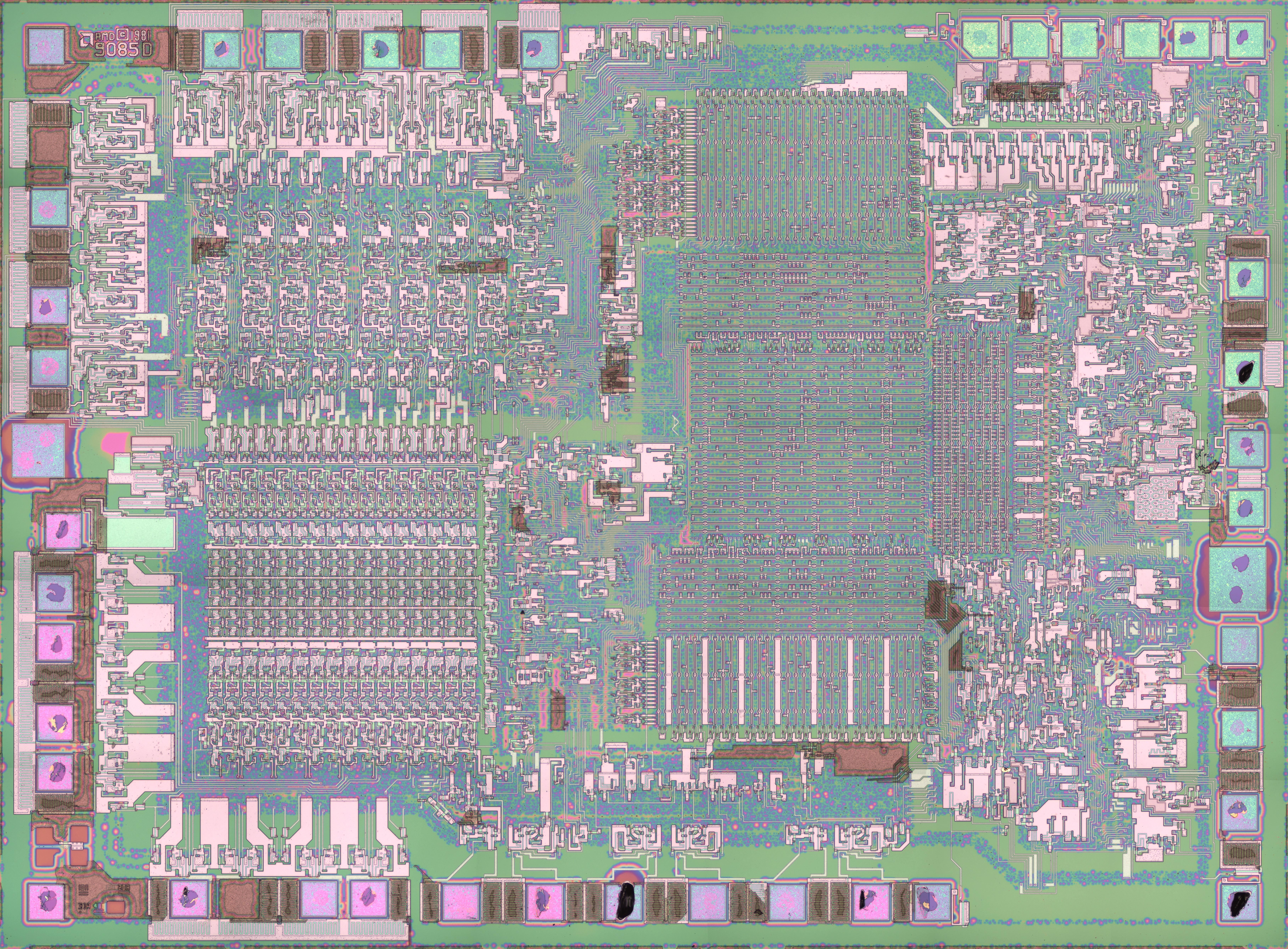
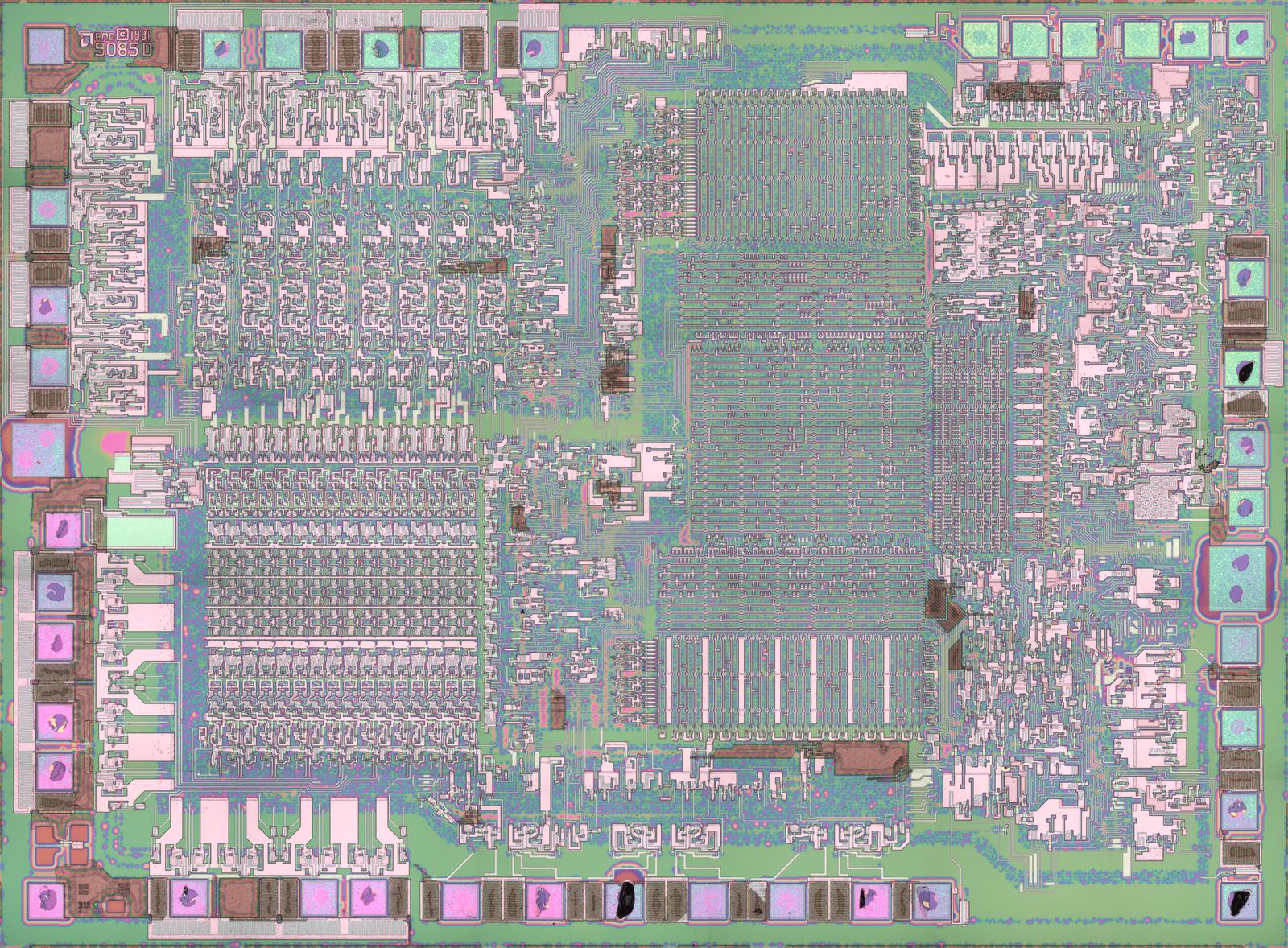
In November, 2012, Christian Sattler delayered the chip and prepared these aligned images of the surface and substrate.
| | 1600 x 1174 JPG 643 kb |
|
|
| | 8638 x 6337 JPG 18.4 MB |
|

| | 8637 x 6336 PNG 272 kb |
|
| | 1600 x 1174 JPG 771 kb |
|
|
| | 8638 x 6337 JPG 12.7 MB |
|

| | 8637 x 6336 PNG 212 kb |
|
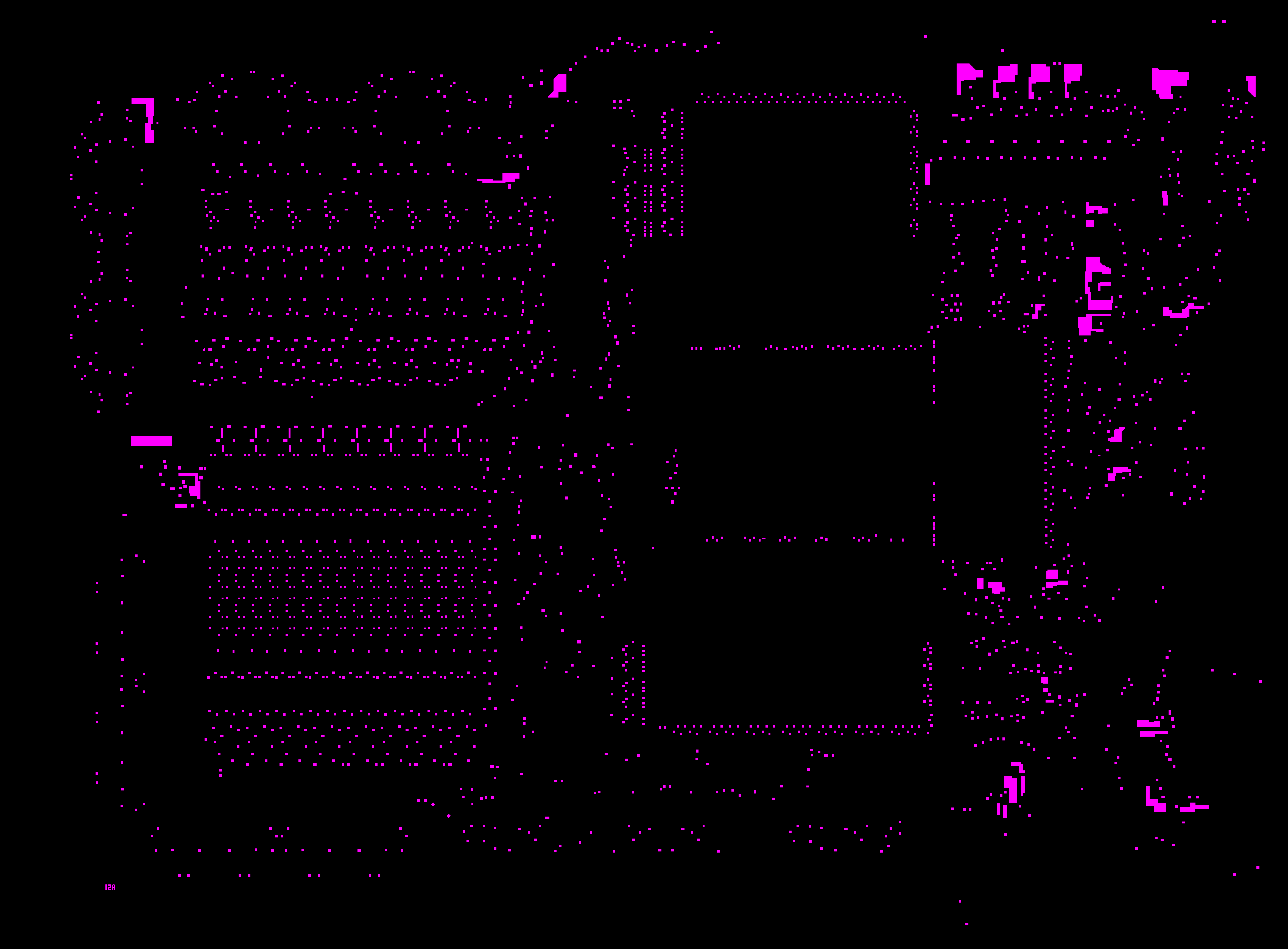
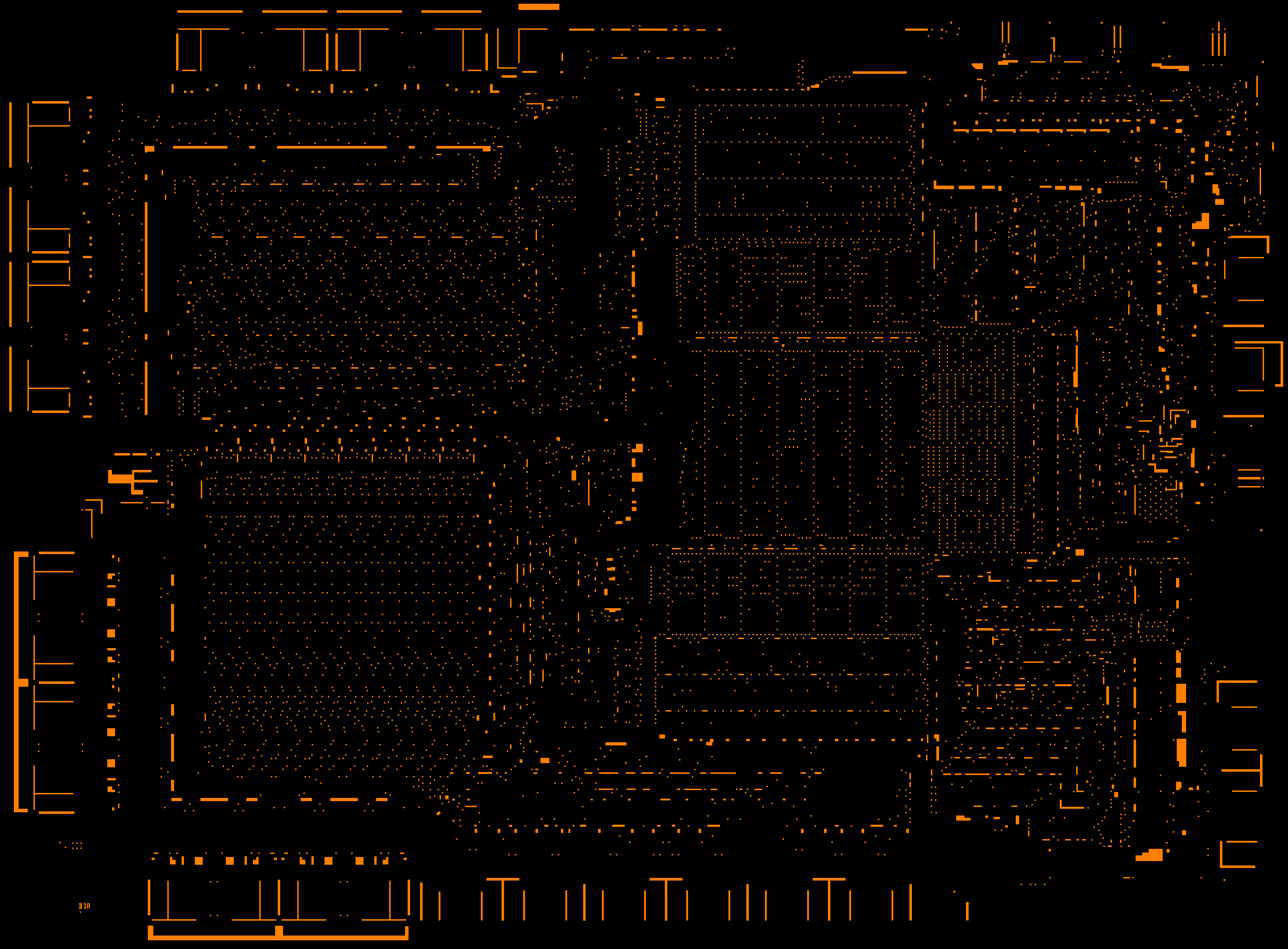
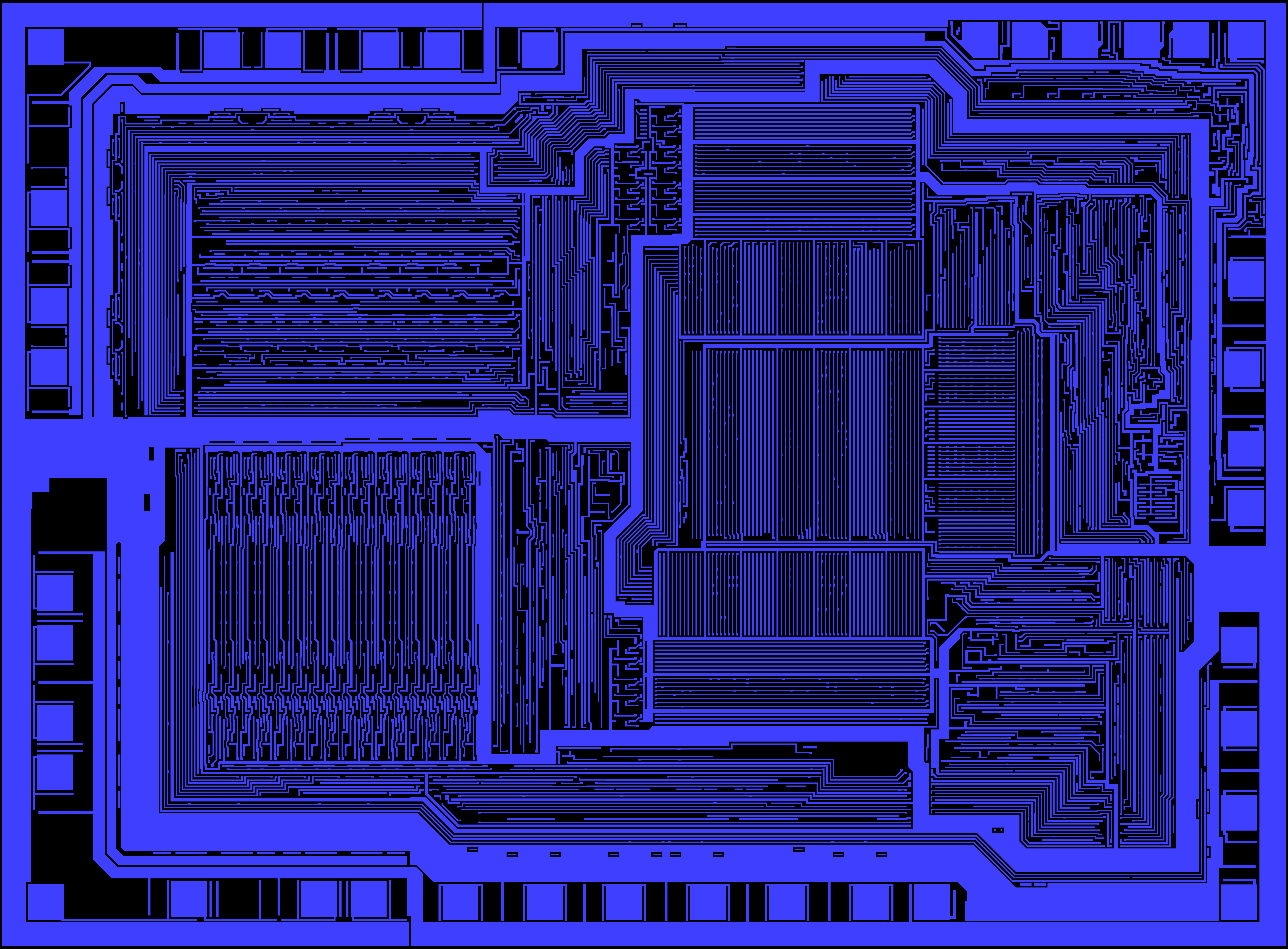
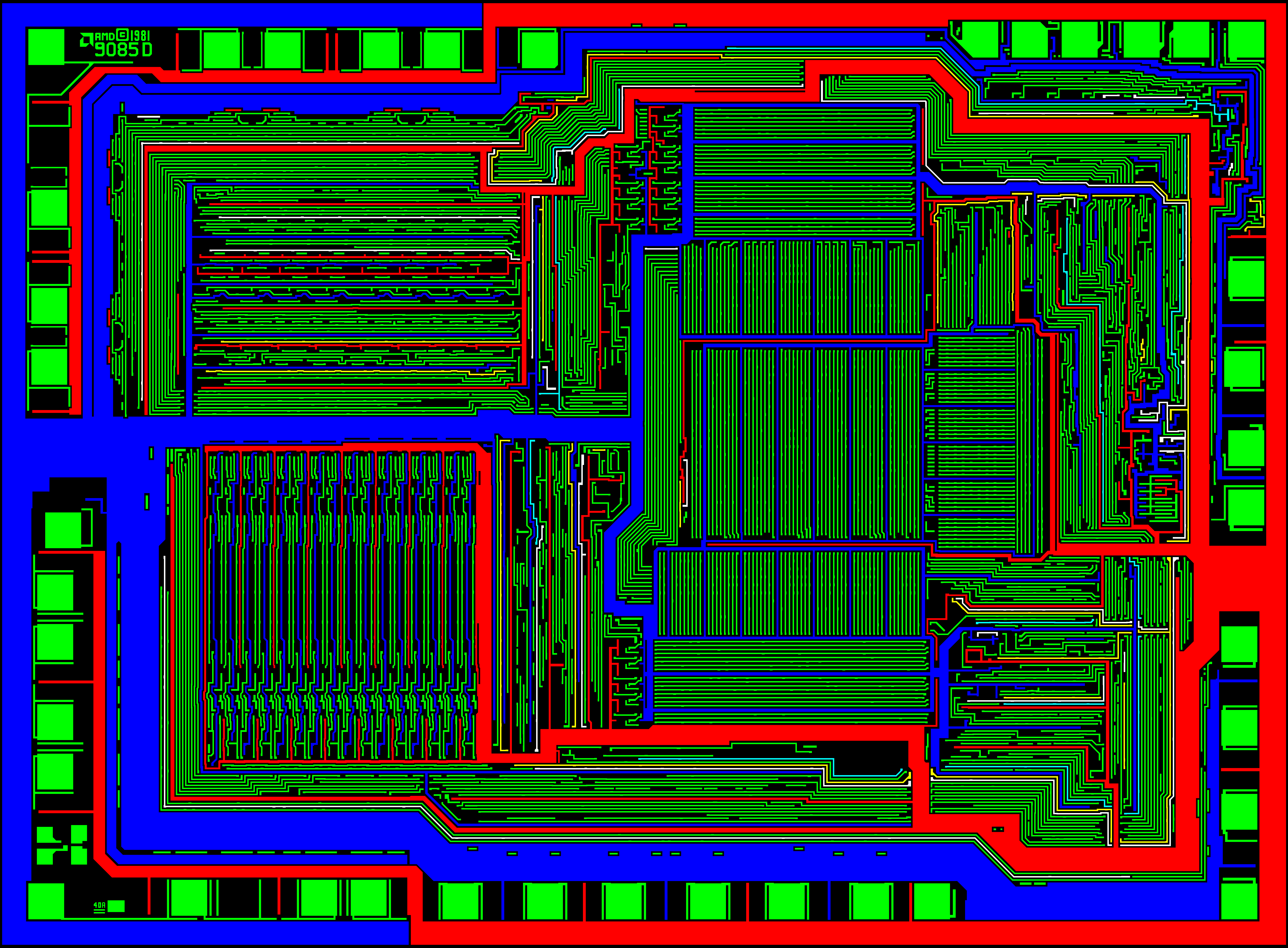
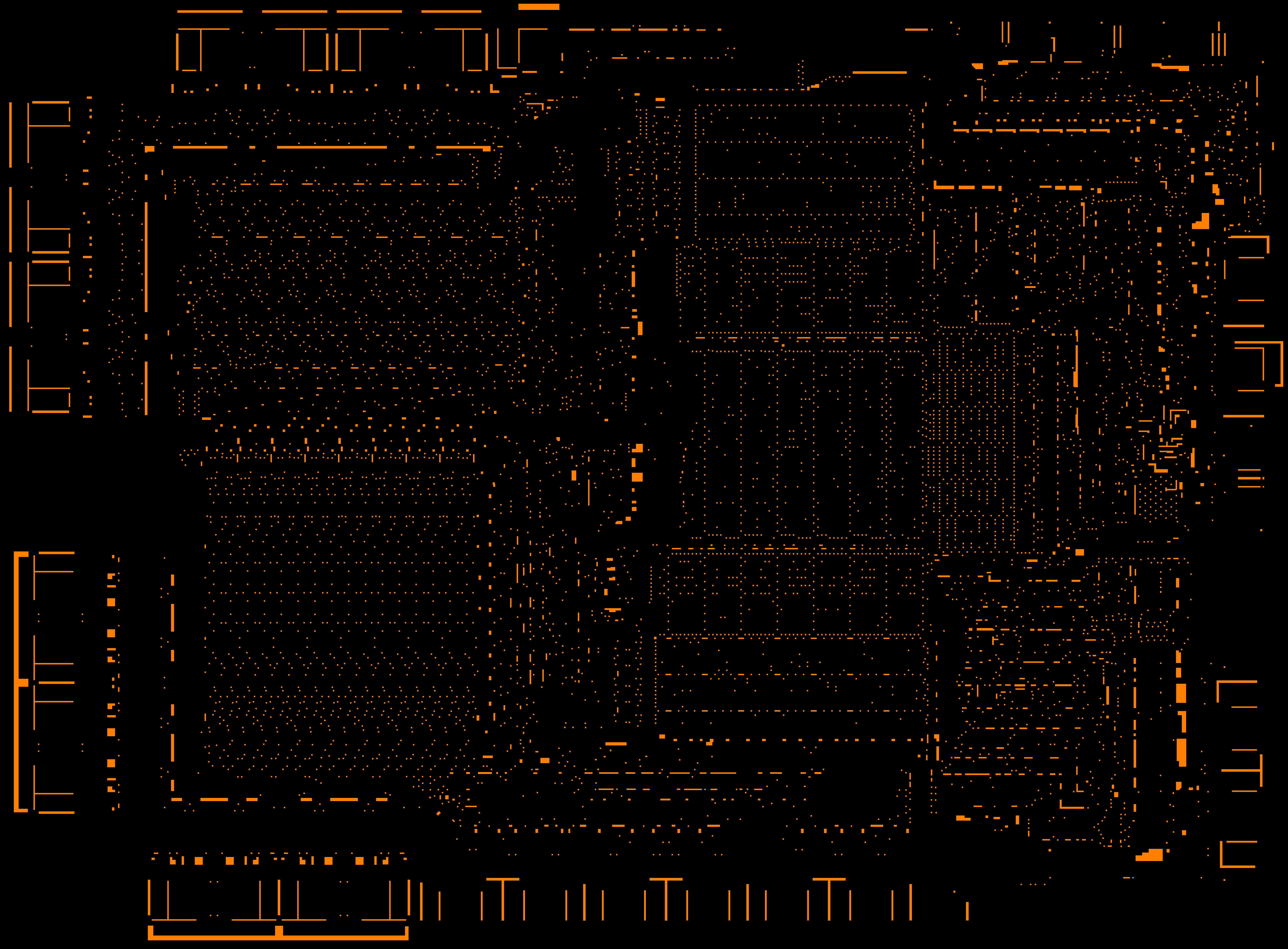
Working from these images, Pavel Zima has built models of each layer, built a gate-level simulation from the layer images, and has brought up his chip model in simulation. Here are his layer images.
To convert the layers for simulation, Pavel removed unused gates and the voltage level shifter. Layers with those features removed and with further corrections found while bringing up the simulation are below.
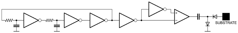
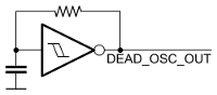
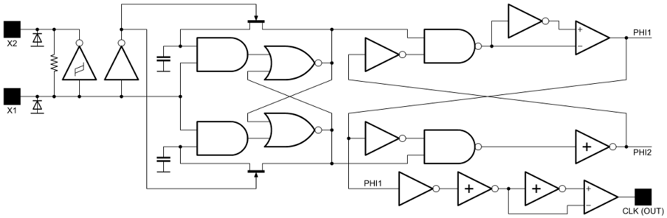
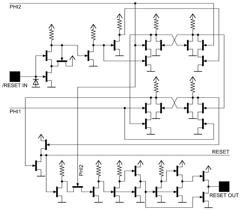
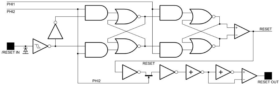
Pavel has also prepared these schematics of the bias generator, an oscillator, the clocks, and reset circuit
If you find these images useful or interesting, please consider a
donation to further our work.


