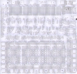
Motorola's 6800 chip was designed before the MOS 6501 and 6502. Many of the 6800's designers left Motorola to join MOS where they produced the 650x series. The chips share the same floorplan, and the 6501 was even pin compatible with the 6800. A lawsuit by Motorola forced MOS to withdraw the 6501, leaving the 6502 with its integrated clock generator as the dominant chip.
The following images are aligned with one another and show the stages of delayering a single 6800 chip. Each full chip image was stitched from about 100 separate microscope shots.
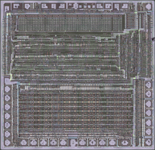
This first image (provided here in two sizes: 1200 pixels wide and 6500 pixels wide) is of the chip surface as we see it after de-packaging the silicon die from its black plastic enclosure. The white traces are aluminum metal, some of which were damaged in the de-packaging process. It is still fairly clear where metal used to be, and as you can see in later images, this will not hinder our reconstruction.
Our first step in de-layering is to remove the metal. This can be tricky, because the entire surface is covered by a clear glass passivation layer which protects the metal from corrosion. Glass is tough, and removing it could damage the underlying polysilicon traces, making them difficult to figure out and model accurately. Luckily, we have a method to remove passivation and metal only from the areas covered by metal, and this has a very low risk of damaging the underlying polysilicon traces. After our process, the chip looks like this:
Notice how you can now see the ROM bits in the top section, because the polysilicon has turned green where it acts like a plain wire and has turned yellow where it forms a transistor. It's also very clear where the metal used to be, so we can resolve anything confusing about the damaged sections in our first image. Our next step is to remove the remaining passivation, which will also erode the underlying polysilicon traces.
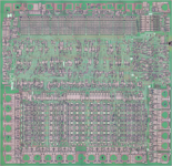
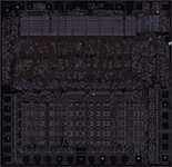
Now the transistors appear bright white, and the polysilicon lines that control them are the light blue-green thin lines. Transistors are formed where the polysilicon lines overlap 'diffusion' areas of the substrate. These diffusion areas are also coming into view because they have some dark blue bands where the passivation was touching them directly. This image was taken with light from a regular halogen bulb shining straight down onto the chip. This is known as 'brightfield' illumination. We can also switch to 'darkfield' illumination where light shines in at a low angle to the surface, accentuating changes in height. Here's the darkfield image:
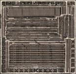
Finally, we strip away the last of the eroded upper layers and clean the surface:
This reveals the bare silicon crystal and gives us a very clear view of the conductive diffusion areas etched into it. The diffusion has narrow channels where transistors used to be and also has many etched spots where vias were carved through insulation to make contact with the metal traces. Between areas of diffusion, the raw silicon is an insulator allowing each region of diffusion to hold a logic voltage independent of the others.
Look for more information and illustrations coming to our wiki soon.
The 68A00P chip was depackaged, delayered, and photographed by Greg James in California's Silicon Valley. Each image was stitched from about 100 separate microscope shots taken with a Nikon LV150 using an LU Plan Fluor 20x objective. The images were corrected and stitched automatically by Christian Sattler in the UK, using Autopano-sift-C and custom code. The full resolution die shots are 10672 x 10309 pixels.
The chip was delayered in February, 2011 and the final substrate image produced on 2/11/2011. If you find these images useful or interesting, please consider a donation to further our work.
